Harnessing the Full Power of the Sun, Part 1 -What exactly is “transparent Cu₂O,” the material poised to dominate the next-generation solar cell market?
2022/09/14 Toshiba Clip Team
- Many solar cells are not fully utilizing the solar energy.
- R&D that would otherwise have been overlooked ended up yielding the highest power conversion efficiency.
- Toshiba begins standardizing the fabrication of a new material to prepare for mass production.
In order to curb the negative effects of climate change—we must develop new technologies that enable the reduction of greenhouse gas emissions to zero. A powerful method for achieving this goal is shifting to renewable energy such as hydroelectric power, solar power, and wind power. As a result, renewable energy generation has been on the rise in Europe; in 2020, more power was generated from renewable energy sources than by fossil fuels for the first time. While hydroelectric power accounts for the majority of this renewable energy, solar and wind power are growing more rapidly. However, solar and wind power have their own limitations—namely, that the amount of power they can generate is dependent on environmental factors such as hours of sunlight and wind conditions.
Therefore, in the case of solar power, there is intense competition around the world to develop low-cost solar cells that can convert sunlight into electricity efficiently during the limited hours of available sunlight. Toshiba has already demonstrated several successes in this area, including the tandem solar cell, which is a combination of two types of solar cells. What combination of solar cells did Toshiba ultimately use to achieve the world’s highest power conversion efficiency and fully harness the power of the sun? A story of trial and error follows.
The fact is many solar cells are not fully utilizing the solar energy
To better understand the significance of the technology that Toshiba has succeeded in developing, we must first touch on how solar cells work. Solar cells are made by layering two types of semiconductors: n-type and p-type semiconductors. These two types of semiconductors are connected by a conductive wire through which electricity flows. When sunlight hits the solar panel, the n-type layer accumulates a negative charge (electrons), and the p-type layer accumulates a positive charge. Electricity is obtained when the negatively charged electrons flow through the conductive wire. As a side note, LEDs (light-emitting diodes) operate by the same principle, but in reverse.
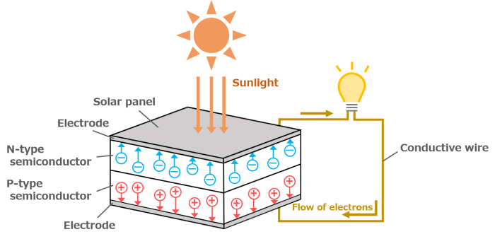
How solar cells generate power
Most semiconductors are made of silicon. Silicon is found in minerals and is easy to obtain and process, making it by far the most cost-effective material relative to other semiconductor materials. However, cost-effectiveness is not the only factor to consider when choosing a material. Each material determines the power conversion efficiency, or how much solar energy can be converted (generated) into electricity. In addition, sunlight spans a spectrum of short to long wavelengths of light, whereas each material can only handle wavelengths within a specific wavelength range.
Even though silicon offers a cost advantage, its power conversion efficiency is currently around 15–25%, which is approaching the theoretical maximum efficiency the material can achieve based on present technology development. This means that there is a limit to how much a solar cell’s power conversion efficiency can be increased if only one material is used. In other words, in order to fully utilize the solar energy, it is important to combine different materials that can convert various wavelengths of solar energy into electricity.
In seeking to pinpoint the right experimental conditions, perseverance is key.
To break through this barrier to achieving maximum solar cell power conversion efficiency, one solution that Toshiba arrived at was the aforementioned tandem solar cell. The tandem solar cell combines two semiconductors with different wavelength ranges and uses them to generate electricity twice, thereby increasing the amount of electricity generated per unit area.
Enter Kazushige Yamamoto of Toshiba’s Corporate Research & Development Center, who has been leading the development of tandem solar cells for about a decade. Yamamoto’s team initially zeroed in on copper indium gallium selenide (CIGS) as a semiconductor material whose wavelength range would not overlap with that of silicon. However, the path to making a CIGS-silicon tandem solar cell a reality was far from smooth. Yamamoto recalls the project’s most difficult days:
“During the first two years, we were able to steadily increase power conversion efficiency using CIGS. Around the third year, however, our results abruptly plateaued… We couldn’t get the results we needed, and the project plunged into crisis. Our research team was reduced to half of its original size, and the members who remained were distraught. I was really ashamed that we had even got the young and promising Shibasaki (to be mentioned later) involved in the whole situation.”
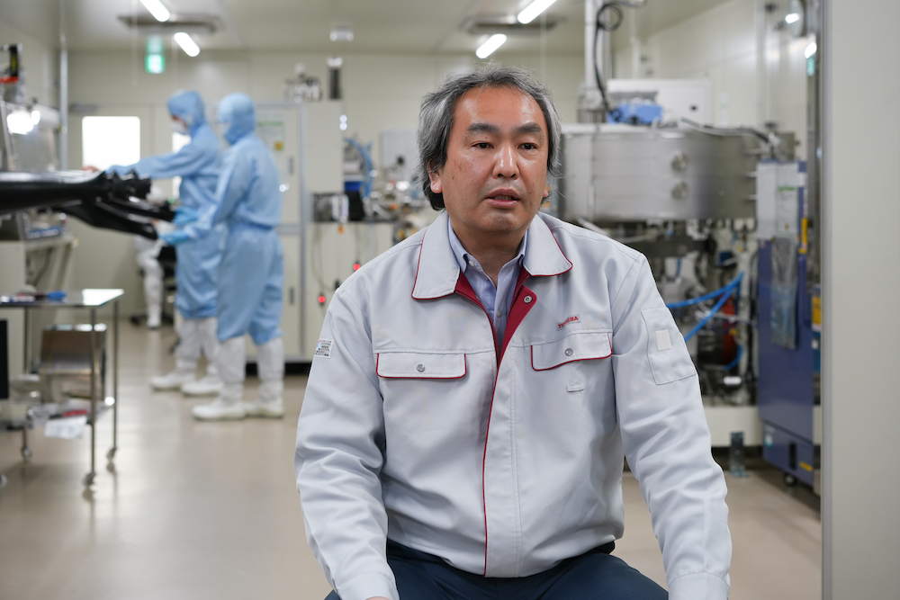
Kazushige Yamamoto, Fellow at Transducer Technology Lab, Nano Materials and Frontier Research Laboratories, Corporate Research & Development Center, Toshiba Corporation
Amidst the somber mood that pervaded the team, a member from another team supporting Yamamoto’s project offered the following suggestion:
— “I know it will take the research back to square one, but why not reconsider other materials?”
This piece of advice spurred Yamamoto to pivot the research toward other materials. The team began to re-explore the potential of Cu₂O (cuprous oxide), which was one of their candidate materials at the outset of research. In fact, when the team was considering Cu₂O on paper in the past, they had been reluctant to pursue further research and development because, in Yamamoto’s words, the Cu₂O that was being researched at the time was a thick material, nearly one millimeter thick, made by heating copper in an oxidizing furnace. Conventional wisdom dictated that it would be impossible to make a thin film of Cu₂O for a solar cell and then attach wiring and other components to make it into a device.
“But we had our backs to the wall, so that didn’t stop us from trying. After all, Toshiba had a veteran engineer, Yamazaki, who had extensive experience in forming copper oxides from his research on superconductors and extensive expertise on film fabrication.
Grasping at straws, we asked Yamazaki to make a thin film of Cu₂O. And, lo and behold, some two or three months later, he handed me a pale orange transparent film, saying, ‘Yamamoto, how about this?’
I knew he was a super engineer, but I remember being completely floored when I saw the transparent Cu₂O film, which no one had succeeded in making before. To make Cu₂O into a film just a few microns thick, every single one of an endless number of conditions during the film fabrication process, such as temperature and oxygen flow rate, has to be just right.
As I found out later, the conditions under which the Cu₂O film becomes transparent are very narrow, and can only be reproduced by those who know them. But most people who attempt the experiment without knowing the conditions will give up before they realize that it’s possible. I deeply admire Yamazaki’s skill and concentration, which has enabled him to pinpoint the exact experimental conditions necessary. He is truly a master of his craft.”
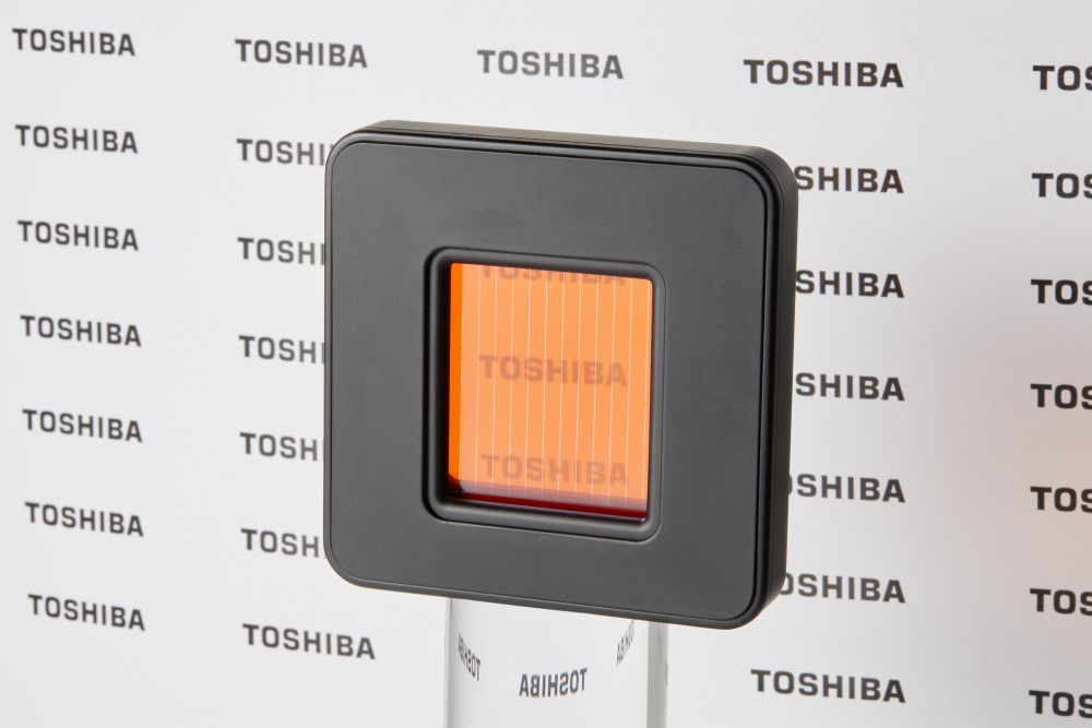
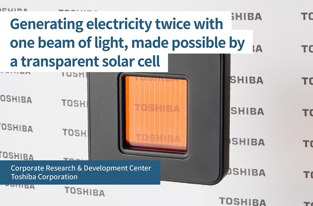
The world’s first transparent Cu₂O solar cell (light orange portion) in a black frame
Creating a solar cell that fully utilizes solar energy, and even surprises a university research lab!
Together with Shibasaki, who was in charge of the physical property analysis, Yamamoto immediately began analyzing and evaluating the thin Cu₂O film that had been given to him. “We provided the evaluation results to Yamazaki as feedback, and through repeated prototyping, we got a good feeling that we could use the material sooner than expected,” says Shibasaki. What, exactly, led them to this conclusion?
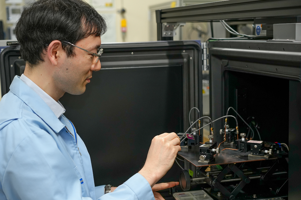
Soichiro Shibasaki, Specialist at Transducer Technology Lab, Nano Materials and Frontier Research Laboratories, Corporate Research & Development Center, Toshiba Corporation
“Cu₂O generates electricity from short wavelengths of sunlight (300 to 600 nm), and because it is transparent, the longer wavelengths pass through it. Meanwhile, silicon generates electricity from long wavelengths of sunlight (600 to 1,100 nm). This means that, because there is no overlap in the sunlight wavelength ranges these two materials need to generate electricity, layering Cu₂O on top of silicon creates the ideal solar cell—the tandem solar cell—for fully utilizing sunlight energy, in the form of both short and long wavelengths.
Even better, Cu₂O is made from copper. Not only is it inexpensive and easy to obtain, but it also has the advantage of being an earth-friendly substance with less toxicity and environmental impact compared to other compounds.”
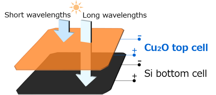
The low-cost, high-efficiency Cu₂O/Si (silicon) tandem solar cell harnesses the energy from sunlight without any losses
Yamamoto adds, “In order to obtain objective evaluation results, we asked a university with an established reputation in Cu₂O research to measure the material’s power conversion efficiency. Not only did they come back with results of at least 2% higher than what was common knowledge at the time, they also asked us, ‘How did you make this beautiful, orange-colored transparent solar cell?’ Their reaction, among and other factors, reinforced our conviction that we were on to something.”
Until that time, research institutes and universities had been trying to generate electricity using thick Cu₂O films made by oxidizing copper. However, no one else had been able to demonstrate a power conversion efficiency greater than 1% using a thin Cu₂O film, and the general consensus at the time was that Cu₂O was not fit for use in a solar cell. In this context, the fact that the team was able to achieve a power conversion efficiency of more than 2% was seen as a remarkable feat. Yamamoto states modestly, “We tried it, and it just happened to work.” Nonetheless, it is a feat that could not have been realized without the determination of Yamamoto and the members of his team, the skills of master film engineer Yamazaki, and the collective strength of Toshiba. They had demonstrated their worth, and the research team was able to regain more members and its former vitality.
Quietly, yet courageously, the team managed to pull off something that no one else could have done. What did Yamazaki, a key member of the project, have to say?
“The Cu₂O film was made by the team, not by me. Admittedly, the deciding factor was my technical sensibility, which is something I can only describe as the first-hand intuition that I have developed through years of experience. However, the results are unquestionably the work of a team that is passionate about creating a product that society needs, and that has charted a course to achieve this goal.”
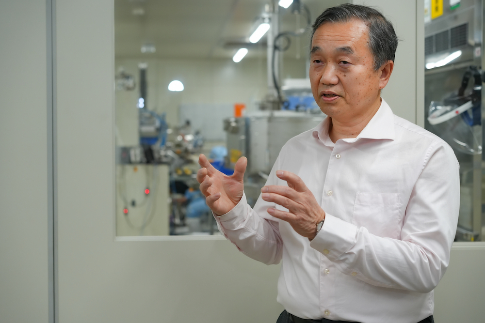
Mutsuki Yamazaki, Transducer Technology Lab, Nano Materials and Frontier Research Laboratories, Corporate Research & Development Center, Toshiba Corporation
Still making strides: Standardizing Cu₂O film fabrication and exploring n-layer materials
The project team is now preparing for mass production, with a target power conversion efficiency of 30% for the tandem solar cell and 10% for the Cu₂O film alone. To get to this point, numerous challenges stand in the way and must be overcome. One such challenge is the standardization of the Cu₂O film fabrication process.
“Further development to raise the power conversion efficiency requires thin Cu₂O films for experimentation. But we can’t make progress if fabrication is completely dependent on the master, Yamazaki,” says Yamamoto. “That’s why several team members apprenticed themselves to Yamazaki to gain expertise and intuition from the ground up, and now everyone can create the film. Now we are moving on to the next stage, adjusting over 100 parameters and steadily preparing for mass production by machine.”
Another challenge was further refining the n-layer. As explained in the beginning, a solar cell consists of an n-layer and a p-layer, with the n-layer overlaying the p-layer—in this case, Cu₂O.
Shibasaki explains: “In Cu₂O solar cells, the focus tends to be on the new material, the thin Cu₂O film. But the electrical properties of its counterpart, the n-layer, are also important. This is because no matter how high quality the Cu₂O p-layer is, if there is a problem with the n-layer, an energetic mismatch will occur at the junction, resulting in a drastic drop in power conversion efficiency.
That’s why, while improving the thin Cu₂O film, we also experimented with multiple n-layer materials in search of the best match. To do this, we had all members of the team study a vast amount of literature, use a variety of simulations, and consider each candidate n-layer material over and over to investigate how each matched up with the Cu₂O layer. We are still continuing this search to further improve the power conversion efficiency.”
The team achieves the world’s highest efficiency of 8.4%, providing momentum for the commercialization of tandem solar cells.
The team continues to make progress. The Cu₂O layer’s power conversion efficiency has improved by leaps and bounds from its initial 2%, and the team achieved a measured power conversion efficiency of 8.4% in 2021. Furthermore, using a simulation, the (estimated) power conversion efficiency of a tandem solar cell that combines this Cu₂O layer with silicon reached 27.4%, indicating that it has the potential to exceed the world’s highest efficiency of 26.7% using silicon alone. This result has provided momentum for the commercialization of low-cost, high-efficiency tandem solar cells.
“Looking back, we have been able to achieve a miracle, but the end goal we have in mind is much further down the road. The power conversion efficiency of Cu₂O alone has not yet reached our initial target of 10%. For it to be used in a tandem solar cell that is practical for society, the Cu₂O needs to be enlarged to the same size as silicon. We also need to establish the process technology for mass production. We still have many challenges ahead,” says Yamamoto.
What challenges lay ahead for the mass production of a Cu₂O/silicon tandem solar cell and for the widespread adoption of such solar cells? In Part 2, we will unpack Toshiba’s technology roadmap and strategy.
![]()
Share this article


