


The impact of an AI that rejects everything but acceptable products -Will it be the savior of digital transformation in manufacturing?
2023/10/16 Toshiba Clip Team
- An innovative AI that identifies only acceptable products.
- Successful testing with world’s largest manufacture of stamped parts for vehicles.
- A trusted reputation rests on a proud record in manufacturing.
Faced with an unpredictable future, one of most-needed abilities in today’s age of VUCA—volatility, uncertainty, complexity and ambiguity—is the capacity for self-transformation. Manufacturers working to achieve Goal 9 of the SDGs, “Industry Innovation, and Infrastructure,” and to “Build resilient infrastructure, promote inclusive and sustainable industrialization and foster innovation,” must expand and streamline industrial infrastructure by promoting digital transformation (DX) in manufacturing.
Despite this strong need, DX is not easy to implement in manufacturing sites that juggle many processes and parts. In such circumstances, AI is expected to be an effective driver of DX, as there are various areas where it can be used effectively. The technology shows particularly high potential in image inspection, where it has proved itself able to perform at the same level as people. Toshiba has developed a proprietary AI image inspection technology using the no-defects learning approach, and is applying it to solutions in Industry, Innovation, and Infrastructure. This article recounts how the AI was perfected and implemented through the stories of two people involved in developing and disseminating the technology.
Companies struggle to conduct product defect inspections with fewer skilled workers
Toshiba’s long history of AI research dates back to the 1950s. AI technologies developed by Toshiba have been used in products such as automatic post code readers and letter sorting machines, and in image recognition processors for advanced driving systems. Nobuyuki Matsumoto of Toshiba Digital Solutions Corporation, which uses AI to support DX in the manufacturing industry, describes the structural challenges facing the manufacturing industry as follows:
“With a growing number of older, skilled workers retiring from manufacturing, the issue of inconsistent quality has become a concern in recent years. The same issue plagues manufacturing processes such as welding, as well as inspections that require workers to visually judge products for defects.
“An AI with capabilities equivalent to those of skilled workers would solve the manpower shortage. If AI were to take over inspections, then the limited number of personnel would be able to focus on higher value-added tasks such as polishing and machining.”

Nobuyuki Matsumoto, Expert, Industrial Digital Transformation Department, ICT Solutions Division, Toshiba Digital Solutions Corporation
To address such challenges faced by manufacturing sites, Toshiba has developed an AI image inspection technology using the no-defects learning approach. The development work was done by Toshiba’s Corporate Manufacturing Engineering Center, which researches and develops production technologies and systems. Yusuke Hirose, who led the development, recalled the original purpose of the project.
“We originally developed it to automate inspections at Toshiba’s overseas plants, where it can be harder to recruit workers with the right skills. We had been studying the main AI algorithm since about 2012.”
Turning common wisdom about no-defects learning on its head
“AI inspection technology already existed. How, then, did Toshiba’s new approach work, and what made it so much better?
IF you train AI on images of known defects, it will not recognize unknown defects. For instance, after training the AI, the manufacturing equipment in use develops a problem that results in a novel defect in products. However, those products are classified as acceptable by the imaging AI, because the defect is not recognized. With skilled workers, the range of defects that occurs during manufacturing might be smaller, which means it is not possible to catalogue all possible defects. However, it is possible for an uncatalogued defect to appear at some time. This is a problem.
Toshiba turned the training process on its head, making it possible to train AI to inspect products using image data of acceptable products only. Put simply, the AI is able to determine the presence or absence of defects based only on the analysis of a model of a good, or acceptable product, against the actual product being inspected. It works by rejecting everything but acceptable products.
Hearing this explanation, one might think, “Why didn’t users just train the AI only on acceptable product image data from the beginning?” Naturally, all companies had the same idea, and AI that exclusively used acceptable product images did exist.
But there was a big obstacle standing in the way: setting optimal rejection criteria. In order to find defective products, a threshold value must be set to determine which products are good and acceptable, and which products fall outside this range and must be rejected as defective. However, if the threshold rejection value criteria are too strict, and the range of acceptable products is narrow, products that would normally be acceptable are judged as defective. By the same token, if the criteria are too loose defective products are judged to be acceptable.
“Finding the optimal setting for the threshold value criteria was the major barrier to practical application,” says Hirose.
Yusuke Hirose, Senior Researcher and Group Leader, Optics & Inspection Technology Research Department, Manufacturing Process & Inspection Technology Division, Corporate Manufacturing Engineering Center, Toshiba Corporation
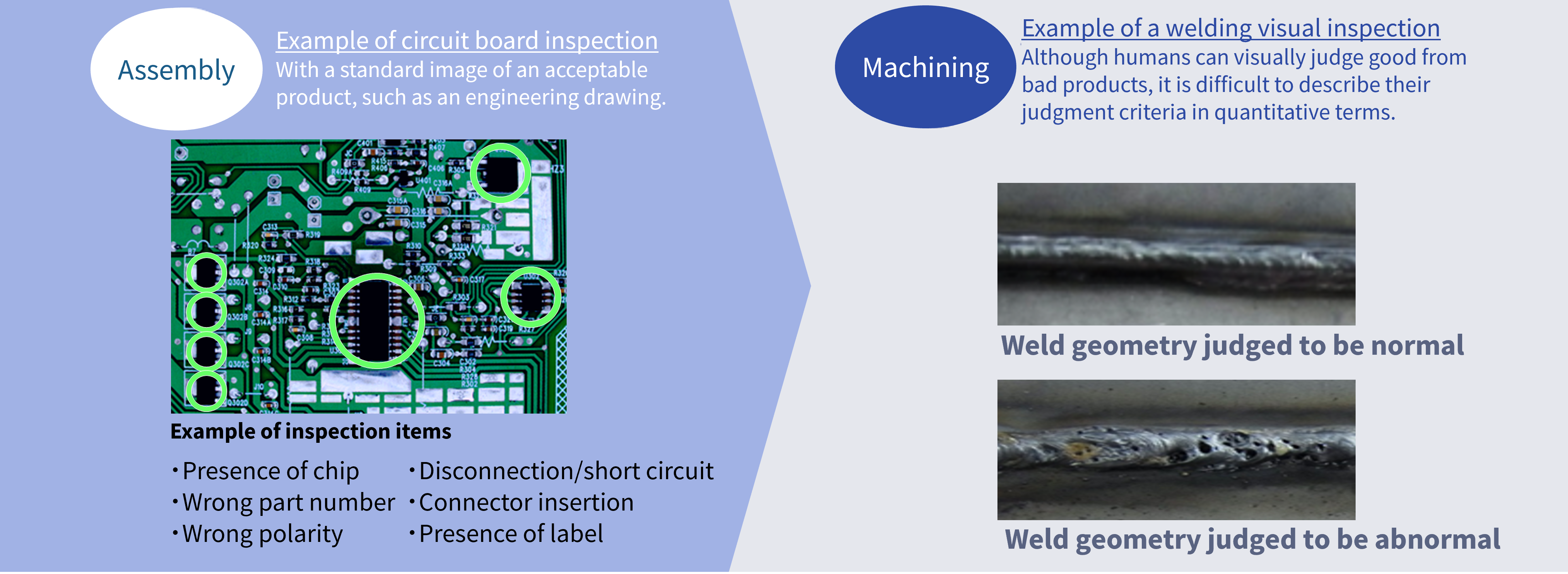
Hirose continued: “What defines a good product in the first place? The settings that form the basis for inspection are where the engineer’s skills shine through.
“It’s easy if you have an engineering drawing, say for a printed circuit board, because acceptable products can be judged by their dimensions. However, in the case of processes, like welding, there may be some variation in the workmanship of each product. For these processes, determining how to set the threshold between acceptable and defective products is much more difficult.
“Furthermore, even products that are considered acceptable will vary in subtle ways depending on the source of materials and aging of the manufacturing machinery. It was quite a challenge to take these subtle variations into account and incorporate them into the AI.”
The threshold value criteria for acceptable products were quantified even for inspections that are difficult to describe clearly in words.
The more difficult the challenge, the more it ignites the imagination of engineers—and that’s what Toshiba is all about. Hirose’s team successfully overcame the problem and applied to patent the no-defects learning approach as a method for reducing misdetection of defects.
“The general approach is to feed the AI entire images of acceptable products. When taking this approach, 3 sigma is the standard deviation used in manufacturing. Sigma describes the degree of variation, and 3 sigma indicates products are judged to be acceptable with a 99.7% confidence level. This is a strict threshold, and there will be cases where acceptable products are judged to be defective.
“So we stopped focusing on training the AI using entire images of acceptable products and sticking to deviation figures of 3 sigma. Instead, to create the AI, we segmented images of acceptable products into smaller parts and trained the AI segment-by-segment. For each part, we checked whether the inspected product deviated from the acceptable range and set the threshold value individually.”
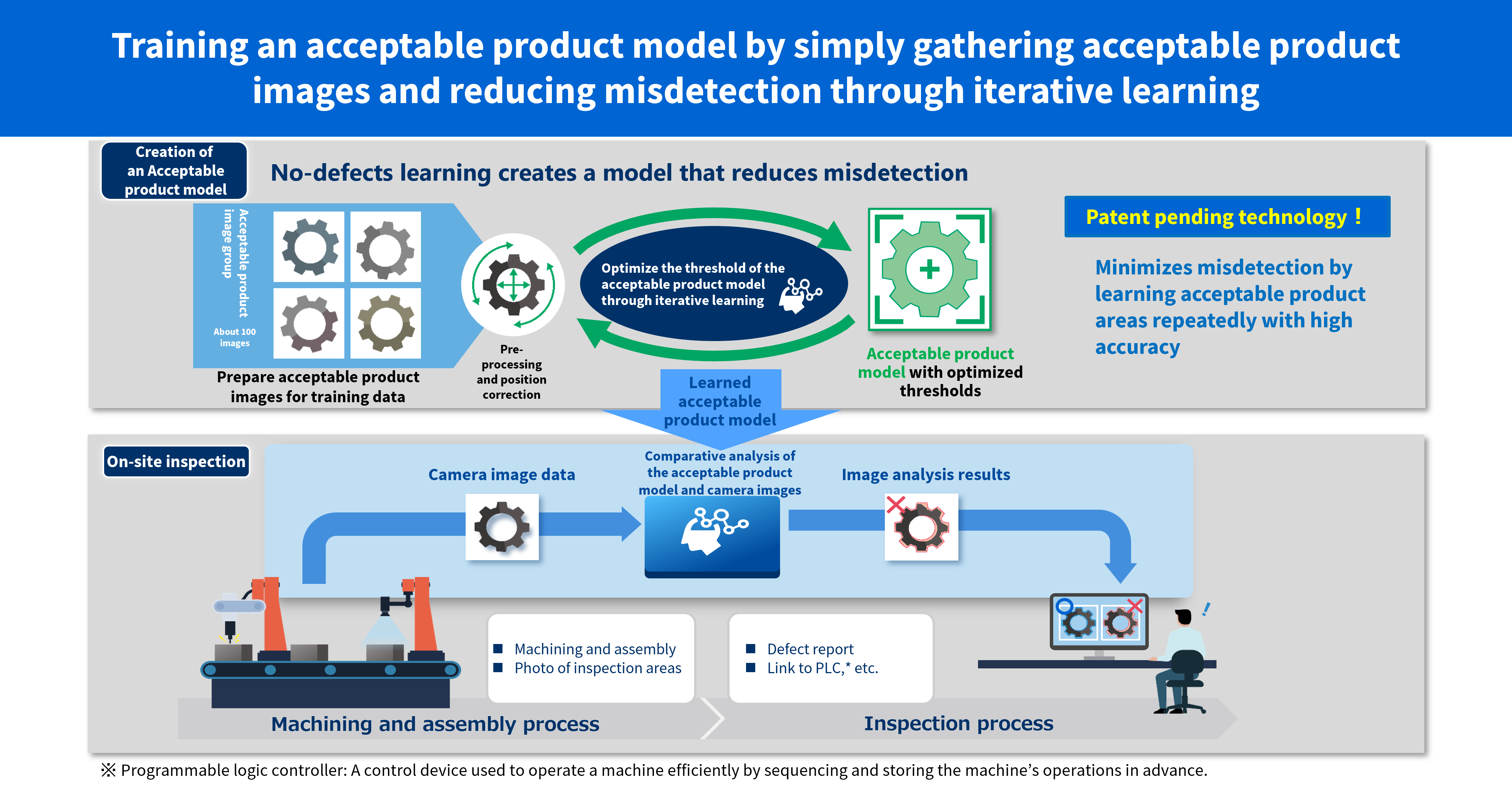
Diagram of how AI image inspection works using no-defects learning
Thus completed, the AI image inspection technology using the no-defects learning approach makes it possible to conduct highly accurate inspections when the AI is trained on data from approximately 100 acceptable product images. If a misdetection occurs and the AI flags an acceptable product as defective, that image can be added to the training dataset, and the AI will iteratively learn and optimize its model by relaxing the threshold criteria. By doing so, the AI will evolve to have even fewer misdetections.
How was all this possible? Hirose emphasizes, “Without a doubt, our deep connection with Toshiba’s manufacturing sites was a key factor in our success.” Hirose and his colleagues, who are also involved in semiconductor manufacturing and other production technologies, have accumulated a wealth of expertise in image processing and photography. Their deep ties to manufacturing sites gave them an intimate understanding of what was required.
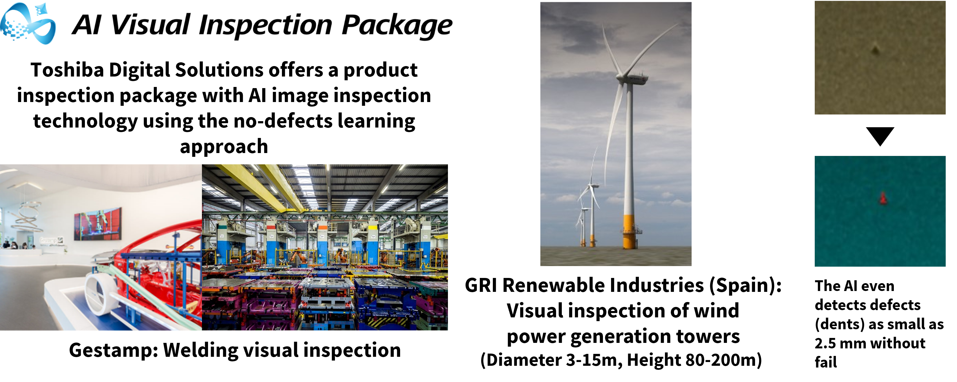
Proof of concept with Gestamp, one of the world’s largest manufacturers of stamped metal parts for the automotive industry
The new AI was initially developed for Toshiba’s own manufacturing sites, but then a turning point came. Industry 4.0, which refers to the digitalization of manufacturing using AI and other technologies, gained momentum around the world, and with it, demand for acquiring and utilizing factory data grew.
Toshiba’s approach was perfectly suited to the times. In Matsumoto’s words, as someone who supports DX in manufacturing, “A lot of manufacturing companies asked for our technology, so we decided to offer up Toshiba’s secret.”
Then the proofs of concept began. An example is the welding quality inspection at Gestamp, the world’s largest manufacturer of stamped automotive parts, with more than 100 plants in 22 countries. Until this initiative, the inspection of defects that occur in the welding process had been difficult to automate. Yet, “in this experiment, the defect detection rate was highly evaluated,” says Hirose. Extraordinary passion and steady efforts were behind this success story.
“We went knee-deep in discussions with Gestamp’s quality personnel about the line between acceptable and defective products. It was a lot of work, but Toshiba’s team was equally determined to create a good product, and I have good memories of the repeated trial-and-error process. Thanks to their help, we were able to create a high-quality system.”
Practical applications of the AI image inspection technology using the no-defects learning approach are expanding
Toshiba’s pride as a manufacturer builds foundations of trust
After successful proofs of concept, Toshiba steered toward commercializing the AI in 2020. The company began offering the AI Visual Inspection Package, a product inspection package that made use of AI image inspection technology using the no-defects learning approach.
Conventional methods of product inspection follow rule-based algorithms. Such systems define tolerance values, then reject as defective any products whose data measured by inspection equipment, cameras, or sensors deviate from the rules. Because there were already many giants in the industry, Toshiba knew that a one-size-fits-all approach would not work in this field.
“To be honest, rule-based inspections are highly competitive because of the power held by major industry players. To differentiate ourselves from them, we had to leverage Toshiba’s strengths as a manufacturer, and find new markets. This was the most challenging part of proposing the AI Visual Inspection Package,” recalls Matsumoto.
What strengths does Toshiba’s AI visual inspection package offer? One is that it does not require a high level of expertise to set up. As mentioned above, all the client company has to do is train the AI on about 100 images of acceptable products. In other words, even without specialized knowledge of AI, it is possible to create an acceptable product model and verify its accuracy by inputting the training images onscreen. This is different from a rule-based system that requires detailed settings.
“Once a manufacturer installs a piece of equipment, it uses it for a long period of time. No matter how brilliant the AI is, it is meaningless if the manufacturer cannot maintain it and use it reliably for inspections over the long term. In this respect, Toshiba has the advantage of being intimately familiar with manufacturing sites due to the trust and track record we have built up over our 150-year history as a manufacturer. We are confident in our AI engineers’ understanding of the do’s and don’ts of manufacturing sites, which is our strength,” says Matsumoto.
Hirose, concluded with these words:
“I have been involved in developing inspection technology ever since I joined the company. When you get down to it, all inspection technology to date simply determines whether a product is OK or not. However, with our AI image technology, it is possible to accumulate a variety of data through both the inspection and image quantification processes. If clients take advantage of this, they will be able to manufacture products more efficiently. Through this technology, we hope to contribute to society in order to realize the SDGs in industry, innovation, and infrastructure.”
Contact Us | Factory IoT Platform | TOSHIBA DIGITAL SOLUTIONS CORPORATION (global.toshiba)
Contact Us | Corporate Manufacturing Engineering Center | Toshiba (global.toshiba)
![]()
Related Links
*This section contains links to websites operated by companies and organizations other than Toshiba Corporation.
Toshiba AI Technology Catalog

Share this article