


Toshiba’s Young Engineers: Taking on the technology, respecting the numbers -Looking at the future of semiconductor manufacturing
2024/01/23 Toshiba Clip Team
- Power semiconductors, a must for carbon neutrality, move to large diameter wafer
- Improving manufacturing capabilities by trial and error – and spending every day with equipment
- Fully understand the site, master precedents. The way to engineer improvement
Recent years have seen power semiconductors move to center stage in the semiconductor industry, and with good reason: as we set our sights on a carbon-neutral future, we can cut energy consumption by improving their performance through technology. In this article, we talk to Tomohiro Taniguchi, who works on improving power semiconductor manufacturing quality and productivity at Advanced Semiconductor Device Development Center. Read about what lies ahead in the evolution of the power semiconductors that support our infrastructure.
Larger wafers will advance manufacturing of power semiconductors, the trump card for carbon neutrality
If we are to reduce CO2 emissions, we must use less energy, and this is where power semiconductor performance determines success or failure—and also explains why they are found wherever electricity is used, including computers, smartphones, automobiles, trains, and power transmission substations. They are essential for the electric vehicles that have contributed to lower CO2 emissions in recent years, and are an indispensable presence in advancing factory automation. As we ratchet up efforts to achieve carbon neutrality, power semiconductors are the focus of global attention.
So, what exactly are power semiconductors? Computers and other electronic devices all dissipate electricity during operation, but power semiconductors act as switches that manage electric power supply, converting between direct and alternating current, raising and lowering voltages, and converting frequencies. As the name indicates, power is electric power, and by controlling its flow power semiconductors play a major role in reducing losses.
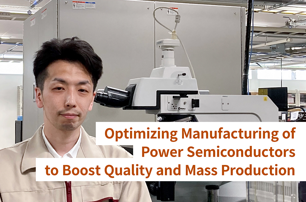
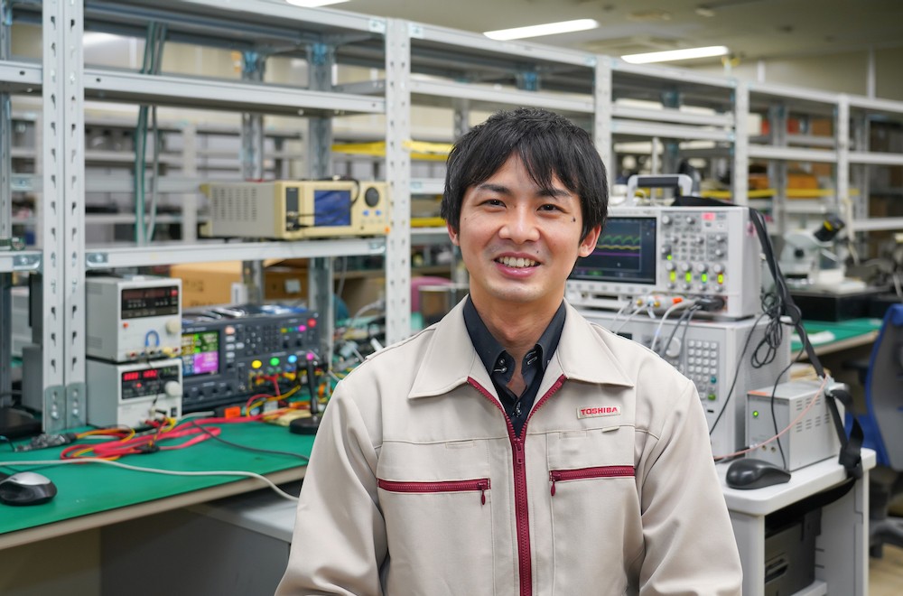
Tomohiro Taniguchi works in power semiconductor manufacturing technology at Toshiba Electronic Devices & Storage. As he explains it, “Our role is to make full use of the latest technologies in stable manufacturing of high-performance power semiconductors. We do this to improve energy savings in a wide range of electrical equipment, and to contribute to the realization of a carbon-neutral future.”
Tomohiro Taniguchi, Specialist, Advanced Semiconductor Unit Process Development Group 3,
Advanced Semiconductor Unit Process Development Dept., Advanced Semiconductor Device Development Center,
Semiconductor Div., Toshiba Electronic Devices & Storage Corporation
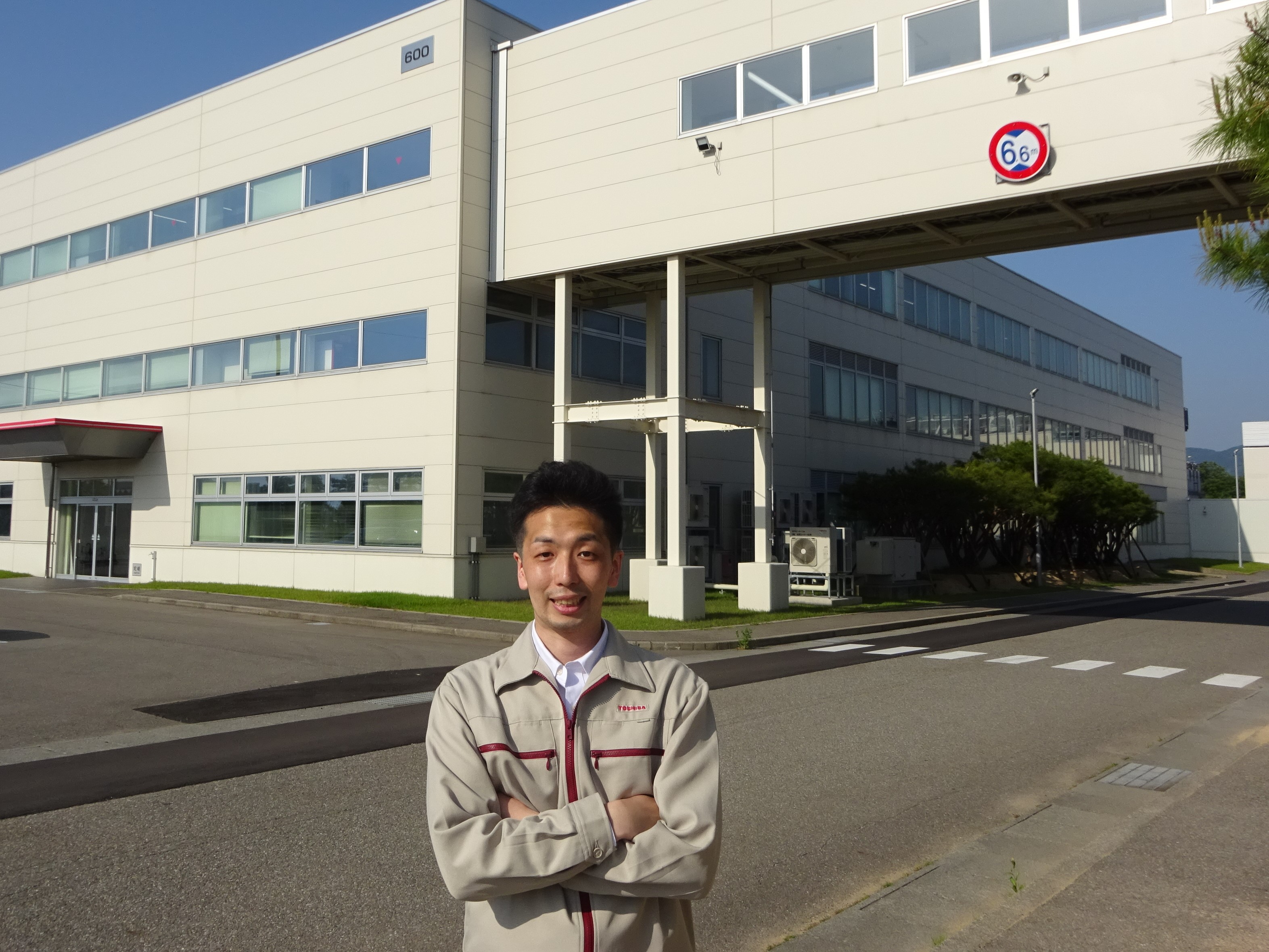
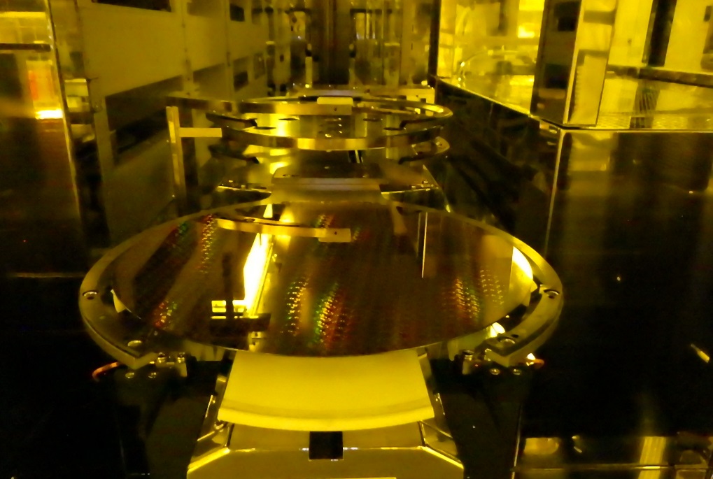
Semiconductors are fabricated on disc-shaped wafers, and increasing wafer diameter is the way to increase power semiconductor production. A larger diameter boosts the number of semiconductors that can be manufactured at one time. Wafers with a 200mm diameter are the mainstream in power semiconductor manufacturing, but in FY2022 Kaga Toshiba Electronics, a manufacturing subsidiary of Toshiba Electronic Devices & Storage Corporation in Nomi City, Ishikawa Prefecture on the Sea of Japan coast, started production on a 300mm wafer line. The company is also advancing construction of a new 300mm manufacturing facility, and aims to start operations in FY2024. Once that comes into play, and first phase operation is in full swing, the company’s power semiconductor production capacity will be 2.5 times that of FY2021. Taniguchi’s department is based in Kaga Toshiba Electronics, and its scope of responsibility covers both development of cutting-edge semiconductors and research and development of manufacturing technologies.
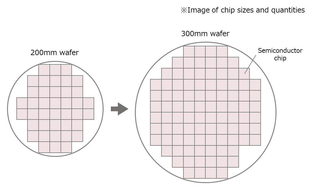
Increasing wafer diameter boosts semiconductor production
“Moving from 200mm to 300mm wafers increases the size 1.5 x 1.5,” explains Taniguchi. “A simple calculation of the area shows that we have a 2.25 times increase in production. So if you ask how Toshiba is responding to the growing demand for power semiconductors accompanying progress towards carbon neutrality and energy savings, the answer is with increased supply capacity. The introduction of production lines that can handle 300mm wafers became an initiative for everybody in our department. Seeing the entire organization working together heightened my sense of responsibility, as well as excitement from being involved in a new technology. Working out how to set up processes using 300mm manufacturing equipment – it’s a project that exhilarated me.”
Memories, such as NAND flash, and CPUs and other logic ICs had already made the shift to production on 300mm wafers. This prompted Taniguchi to approach colleagues who had experience of the transition and pick their brains. The history of Toshiba’s semiconductor business spans over 60 years, and in that time it has built up innumerable tangible and intangible technological assets, along with a culture of friendly rivalry among engineers. The same countless personal commitments that took semiconductor performance and mass production efficiency to the world-class level provided strong support for the start-up of the 300mm wafer line.
It’s not just larger wafers—introducing new technologies excites engineers
Semiconductor manufacturing comprises multiple processes, including deposition of thin insulating films and metal films on the wafers, fine levels of lithography to form circuit patterns, and finally dicing, use a diamond blade to carefully cut out the individual ICs on the wafer. Mr. Taniguchi is part of a group that specializes in metal-film deposition, and he has worked as an engineer on the optimization of the deposition process against manufacturing requirements. He is also responsible for development to support stable production, and is devoted to improving technology.
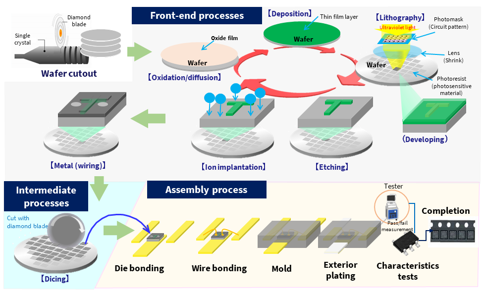
Semiconductor manufacturing involves numerous processes
“You cannot simply apply 200mm wafer processes to 300mm wafers,” says Taniguchi. “When you use a larger wafer, there is much greater potential for increased process variability. For instance, in the deposition process, conditions must be adjusted to ensure uniform film thickness from the wafer’s center to its edge. Our approach to quality control is not just to rely on our own technical knowledge but to combine it with the know-how of manufacturing equipment manufacturers, to raise the level of achievement.”
Equipment performance is crucial in semiconductor manufacturing. It has an immense impact on production efficiency, and on product quality and performance. The manufacturers regularly update specifications, and semiconductor engineers have to keep up with the changes. On top of this, making decisions on equipment purchases is no small thing, as a single item can range in price from millions of dollars to tens of millions. Questions about how much to invest and what kind of equipment to purchase to realize more stable production and higher quality are the sort of things that really engage engineers.
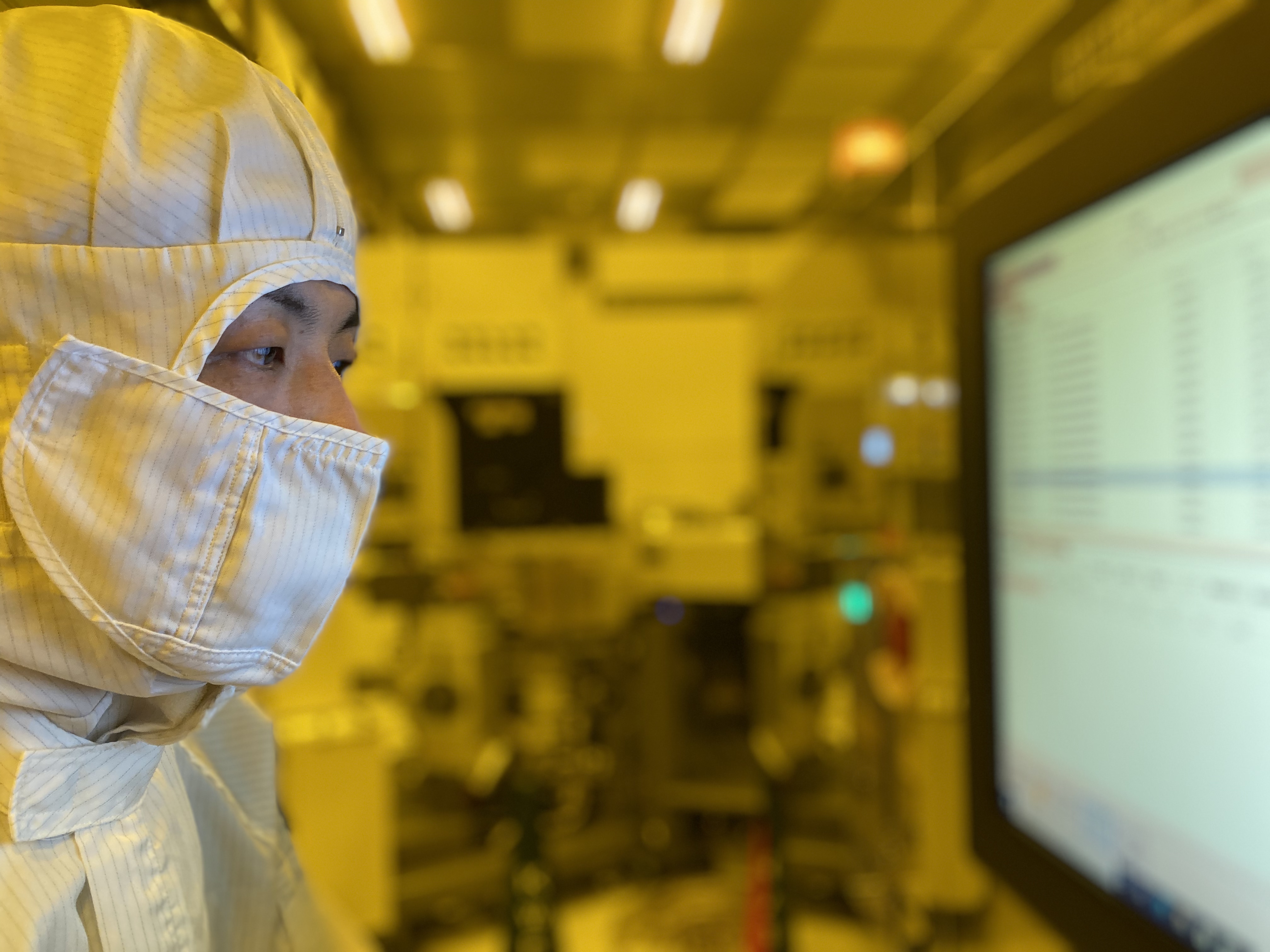
Taniguchi knows all about this. “Investing in equipment is front and center in power semiconductor manufacturing, and there is a strong sense of excitement about pioneering technology. You ask yourself if there is a way to increase the productivity of the equipment, to manufacture more power semiconductors, and improve the quality…I’ve spent all day in a clean room fine-tuning the movement of the wafers and devising ways to stabilize the temperature. I got really excited when, after a lot of trial and error, I managed to adjust the conditions to get stable production.
I want to raise my technical level and become an even better engineer. That is why I continue to give it all I’ve got. Think, plan and execute experiments… Try things, adjust course based on the results, and then try again. It’s a slow, and repetitive process, but the moment an experiment goes according to plan and a problem is solved, I feel a sense of satisfaction as an engineer. It’s a real pleasure, and I want to experience it more.”
Let’s imagine that, thanks to Mr. Taniguchi’s efforts, a machine that processed 100 wafers in an hour can now process 150. Semiconductor production lines operate 24 hours a day, 365 days a year, which means that even if an improvement is small, an accumulation in processing capacity can push up production capacity. Taniguchi is keenly aware of this: “We are constantly probing for ways to improve the numbers.” The aim to increase supply capacity and increase power semiconductors production. And beyond that vision, there is concern for eco-friendly electrical equipment and a sustainable society.
Understand the production site, learn from precedent. Improve as an engineer
Taniguchi has strong convictions about his work. “I believe it is important for engineers responsible for optimizing the deposition process to know the equipment at the manufacturing site and to know the past,” To his way of thinking, the only way to understand the real value of manufacturing equipment is to look at the drawings and see how it actually works. When the 300mm wafer manufacturing equipment was introduced, he got the manufacturer’s permission to observer it carefully, to check it out hands on, to try to really understand it. Another thing he does in attempting to unravel the technology of semiconductor manufacturing is to never forget to understand how his predecessors solved problems.
“I don’t think you can really utilize new manufacturing equipment and improve process productivity unless you keep a close eye on it once it’s on-site. I sometimes come up with ideas at random moments, like when I’m taking a bath or lying in bed. I think it’s because I constantly observe, and somewhere in my subconscious my thoughts are still turning over.
“Knowing the past means I don’t waste time reinventing the wheel by trying to develop technology without looking at what already exists. When dealing with the challenges at hand, we need to be familiar with our own cumulative expertise, and to keep an eye on technology trends in the industry.”
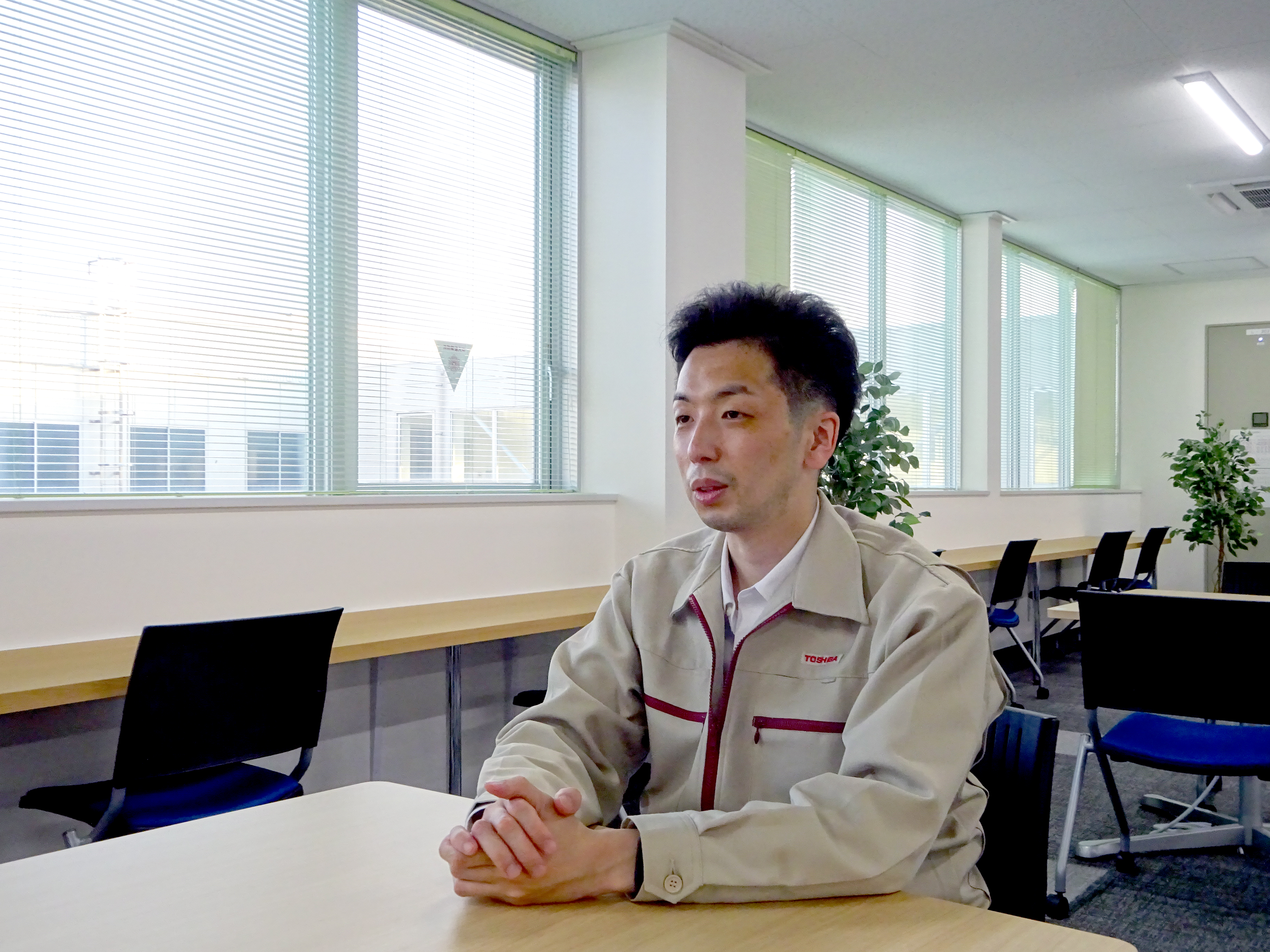
Taniguchi in the clean room, adjusting processing conditions for manufacturing equipment
Really familiarize yourself with the site and learn from technological precedents – underpinning this creed is Taniguchi’s conviction that “work is done at the manufacturing site and engineers must complete it themselves.” Mr. Taniguchi’s experience has allowed him to grow as an engineer.
“In my third year with the company, I had the chance to visit an equipment manufacturer, by myself. I was there to see a trial run of a new technology they proposed to adopt on a film deposition line and what kind of results would be obtained. Having run several simulations, I headed to the factory with some degree of expectation for the results, but…”
The experiment produced numbers that differed from the plan, and there were unexpected problems. Taniguchi was confused, and called his boss to consult with him. Once he had proper instructions, the trial was finished without any more hitches. But what Taniguchi remembers even more clearly was the message from his boss: “Think about the significance of being there on-site as a Toshiba engineer, and make sure you complete the experiment properly before coming back. If you can’t handle things on the spot, there’s no point in sending you on business trips.” The message remains etched in Taniguchi’s heart, and he still thinks about its meaning.
“’If all you want to look at is experimental numbers, maybe all you need to do is send samples and exchange data. Even if we get unexpected figures or problems come up, we work it all out at the site.’ That was the true meaning of his words. In the preliminary simulations, I might well have put too much emphasis on numbers… It is essential to seek out the knowledge of one’s superiors on the technical side, but you also need to be thoroughly prepared, and that includes what to do on-site. It was through this experience that I think I acquired the attitude of an engineer.”
Taniguchi has learned a lot and can stand tall as an engineer. While continuing to demonstrate strengths in process management and productivity improvement, he is enthusiastic about running new projects, such as the 300mm wafer line. Asked about his thoughts on Toshiba Group’s “Our Values” he replied without hesitation, “Do the right thing.”
“We must continue to do the right thing with technology. Carry out experiments based on solid technologies, and accept the numerical values and results obtained as facts. There should be no room for bias or conjecture. As long as we do the right thing with the technology, the output will be honest. And if the products we make are honest, they will be good for society as well. Only if each and every engineer does the right thing will our Group message shine: “Committed to people, committed to the future.”
![]()
Share this article