


How to make semiconductors, the brains of everything
2021/02/10 Toshiba Clip Team
Smartphones, cars, toys. Semiconductor products are used wherever electricity is used. You could say our lives would not be possible without them. Do you know how these semiconductor products are formed, or how they are made?
In this article we will tell you all about the world hidden away in the black plastic of semiconductor packages.
The nanometer scale map that covers silicon chips
Electric products consist of numerous components. The parts where processing and operations are performed by a flowing current of electricity are the electrical circuits, made up of elements like resistors, diodes, transistors, and capacitors, and the wiring that connects them. Making these elements of circuits smaller, making the wiring thinner and shorter, and minimizing electrical circuits that perform the same operation, is called integration.
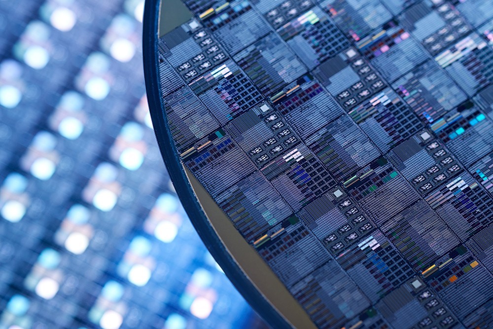
On an integrated circuit or IC, a part of semiconductors, innumerable electric circuits are formed on a chip of silicon. They are so small and so densely integrated that they are invisible to the naked eye, but they spread out over the silicon surface like lines on a map.
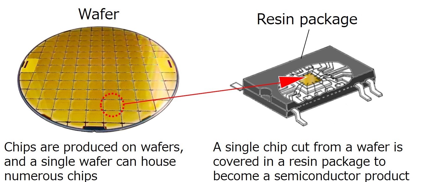
The chip manufacturing process has two phases: front-end processes, where the chips are formed on wafers, and back-end processes, where the finished wafers are cut and chips are housed in their packages
So how are these silicon maps made? Let’s take a look at the main processes.
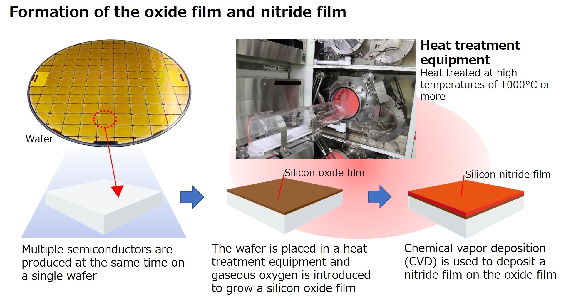
First, an oxide film is formed on the surface of the wafer by heating it to a temperature of about 1,000°C.
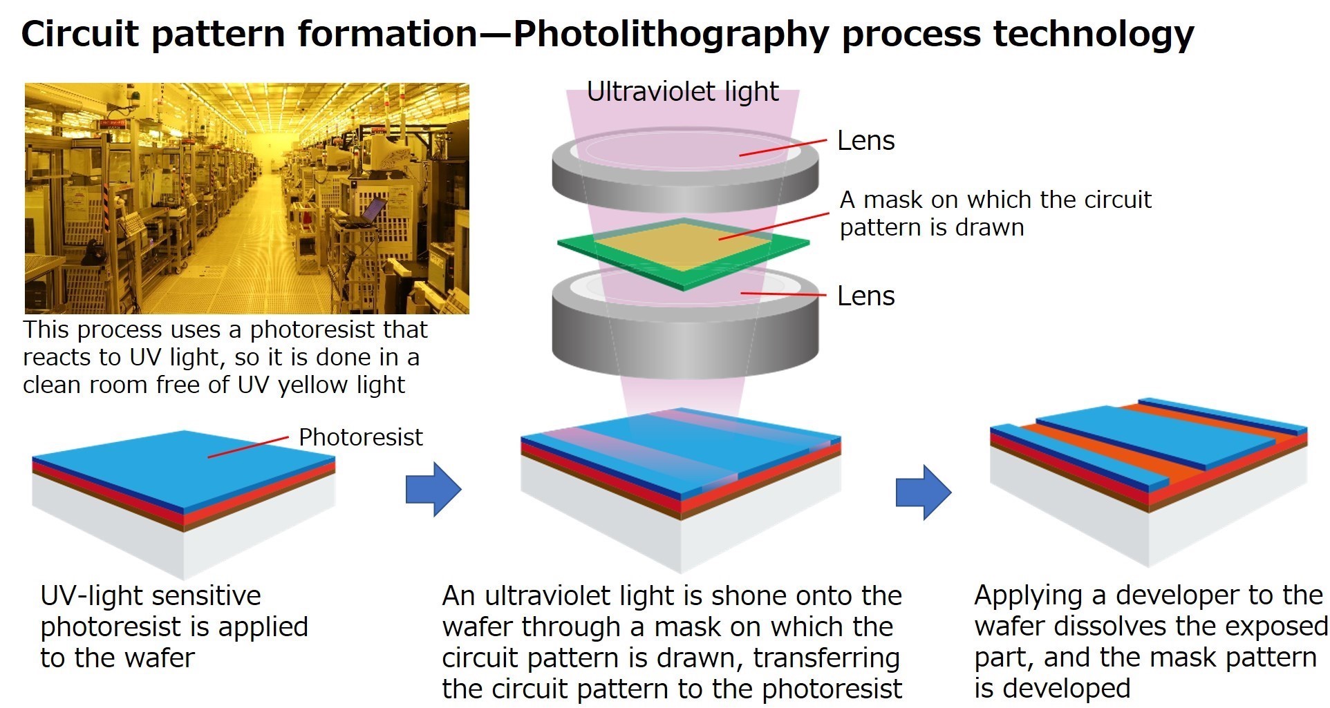
Electric circuits comprising minute elements and wiring, are made on the wafers on which this oxide film is formed, but the secret to achieving minimization of the electric circuits lies in light.
At this stage, photoresist, a substance that undergoes a chemical reaction when exposed to ultraviolet light, is applied to the oxide film. A beam of light is then applied to the chips on the wafer, via lenses and a glass plate, known as a mask, on which a circuit pattern has been formed. The photoresist is exposed to the light, and the pattern for the circuit is transferred to the wafer.
The next step is an etching process to remove unwanted photoresist and oxide film. This is typically wet etching that relies on a reaction to a chemical solution to leave only the photoresist forming the circuit. There are also dry etching methods that typically use gas, plasma or ions to carry out specific chip processes.
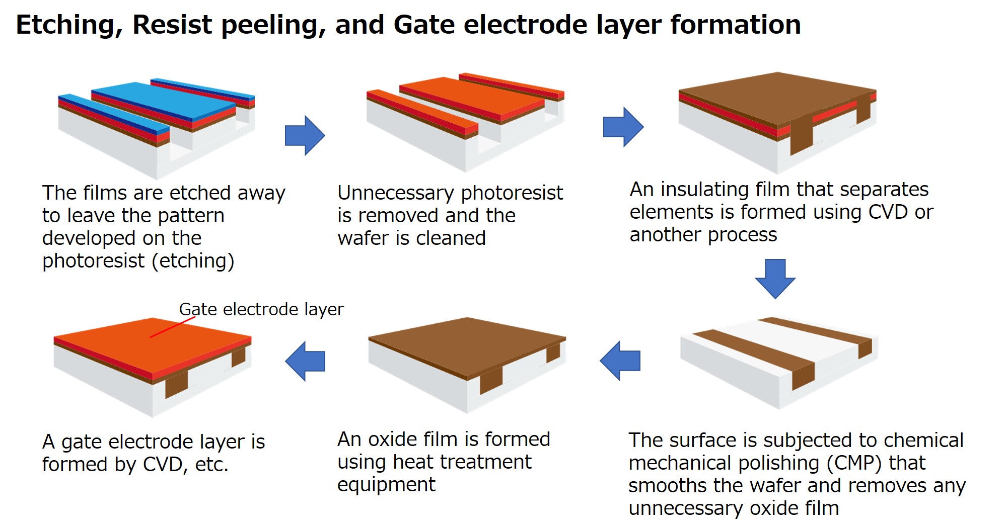
In a process known as doping, impurities, such as boron and phosphorus ions, are introduced into the wafer on which the circuit patterns have been developed, completing the creation of intermediate substances between a semiconductor that conducts electricity (conductor) and one that does not conduct electricity (insulator).
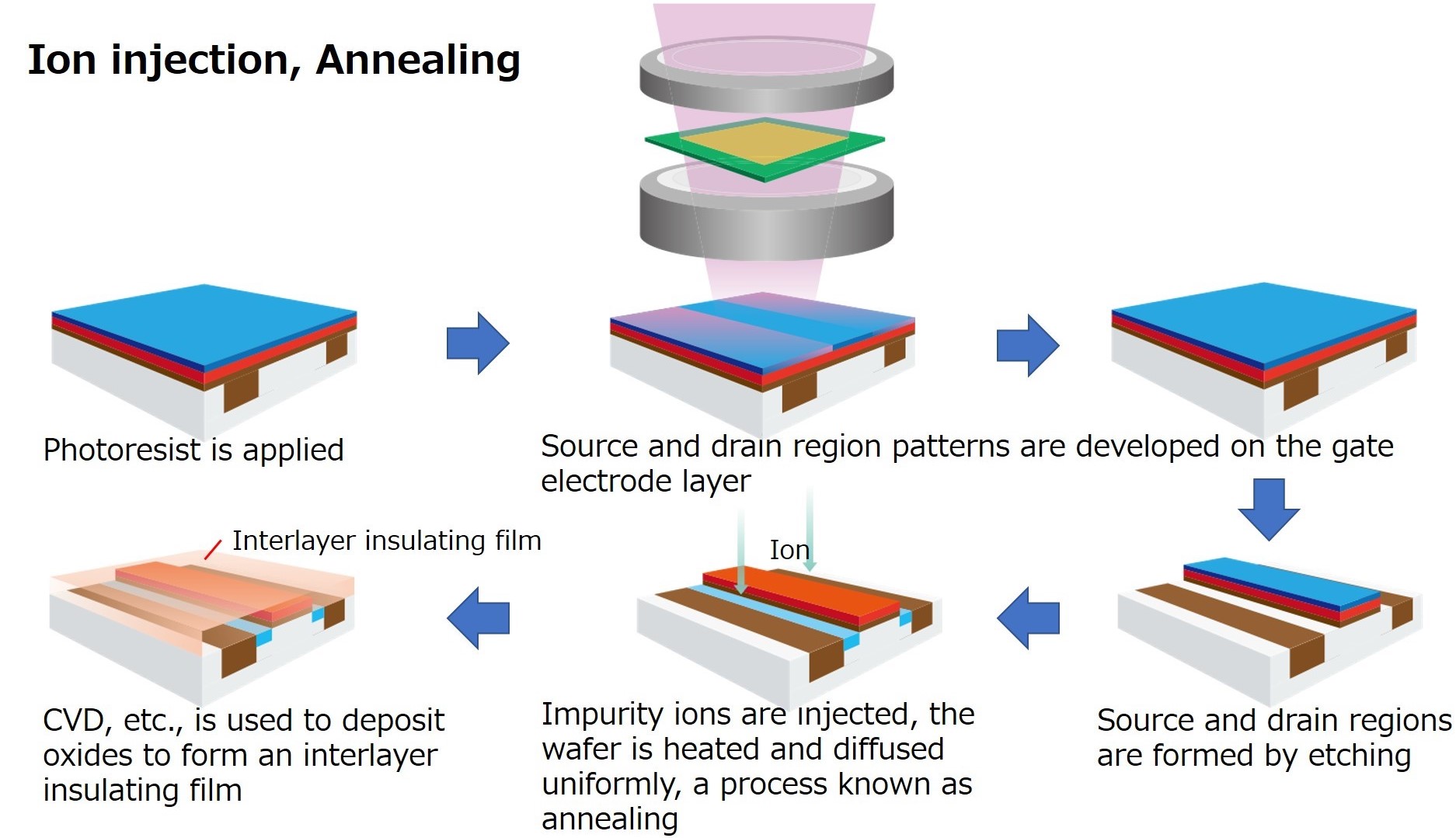
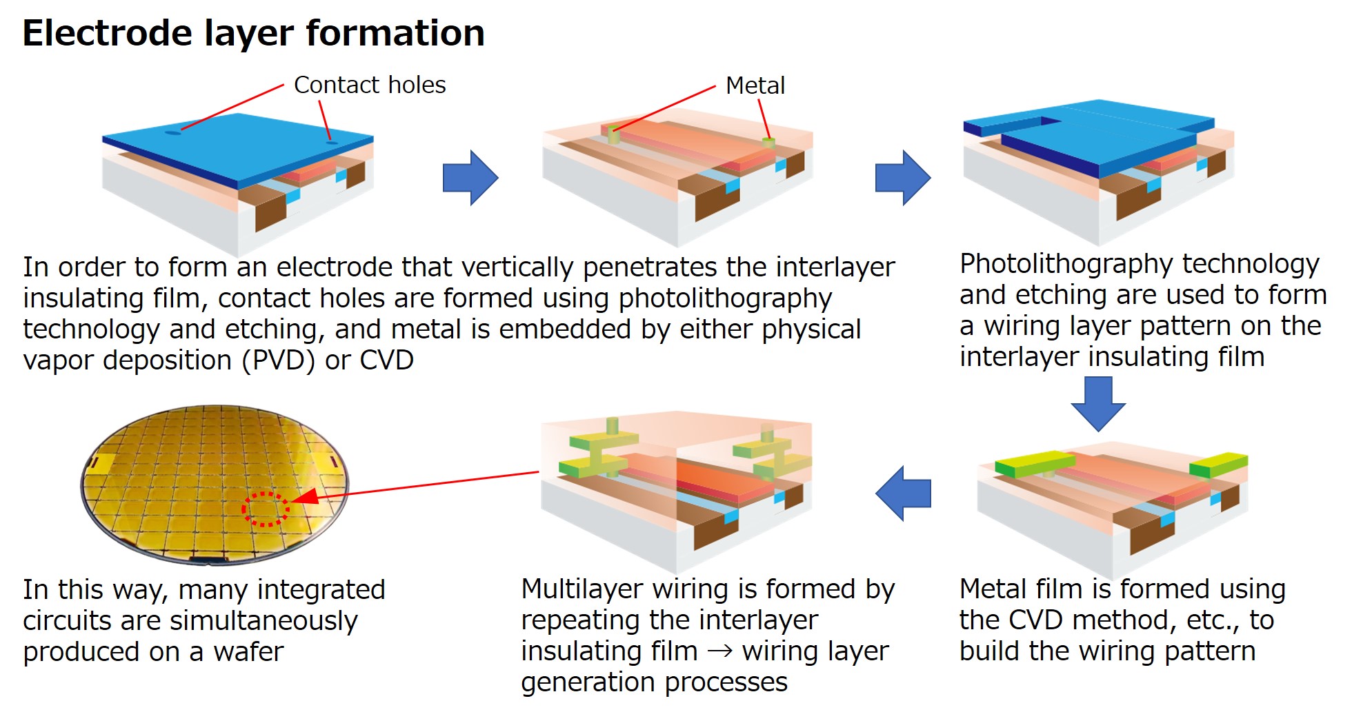
By combining and repeating these steps, the desired elements are formed on the silicon wafer. Then, by forming a metal film for wiring that connects these elements, the circuit is completed, and finally an integrated circuit is made.
Air cleanliness determines the final quality of a semiconductor
With all front-end processes complete, wafers move on to back-end processing, where individual chips are cut from the wafers and encased in resin packages prior to shipping.
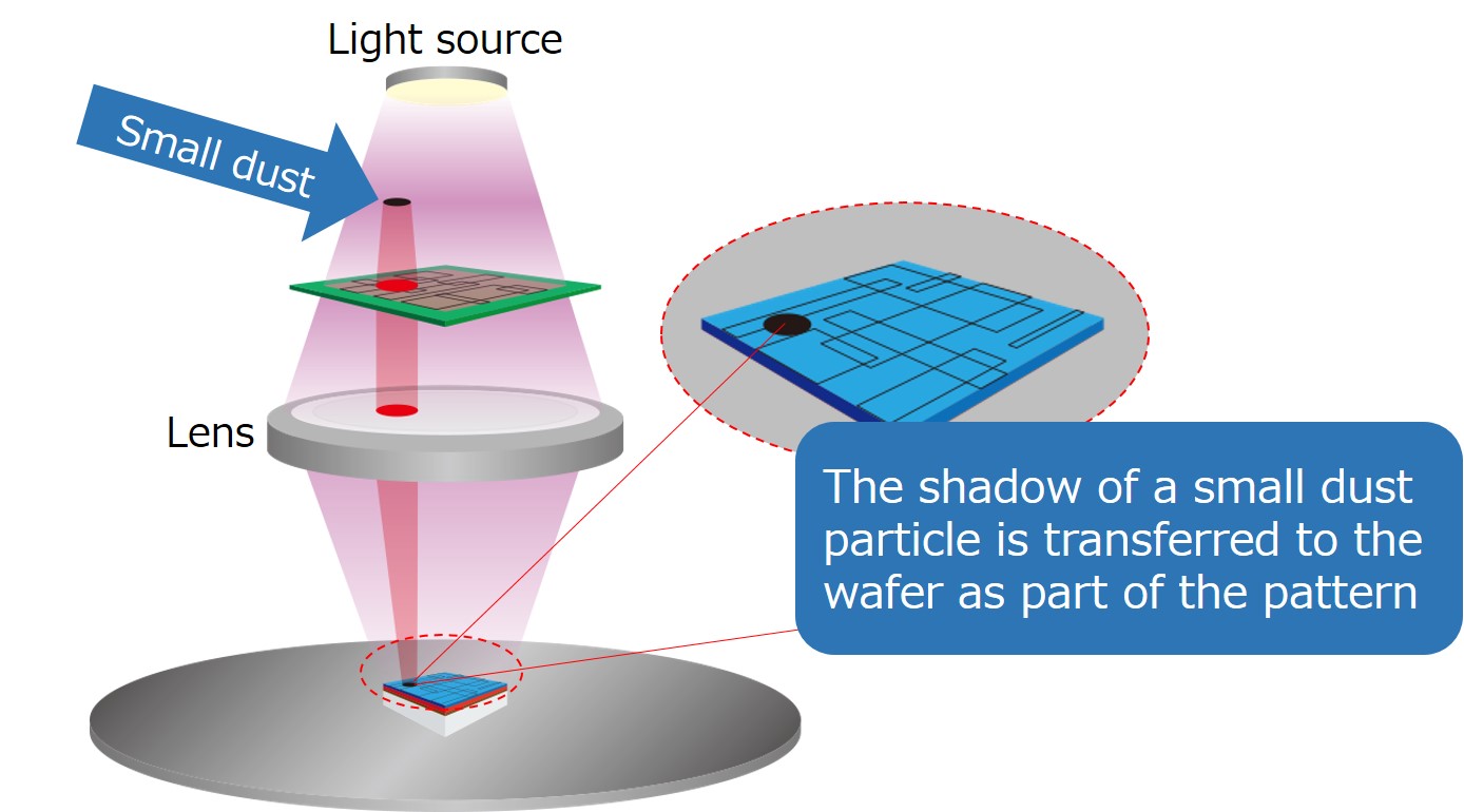
Front-end processing work is on the nanometer scale, the billionth of a meter level, and it is impossible to check and confirm results with the naked eye. After completion, wafers are subject to stringent inspection and quality checks.
The single-most important factor in determining the pass rate is air cleanliness.
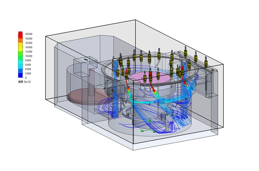
Consider, if photolithography of the circuit pattern is done in an environment where there are dust particles floating in the air, their shadow may be transferred onto the wafer, as in the figure below. In some cases, dust can also interfere with etching meaning unwanted parts cannot be removed correctly, resulting in failing quality inspection.
Semiconductor manufacturing sites require a pristine environment in which ambient dust is at the absolute minimum, so for this reason production is done in a “clean room” with specially raised air cleanliness.
If minute particles of dirt or dust are in the air…
A clean room keeps its air clean, and the degree of cleaning is controlled from inside and outside, to prevent the intrusion of dust.
Air inside the room flows from the ceiling to under the floor, or to suction ports on the wall, where it repeatedly passes through high performance filters that capture any dust. The air circulation system returns only cleansed air to the clean room.
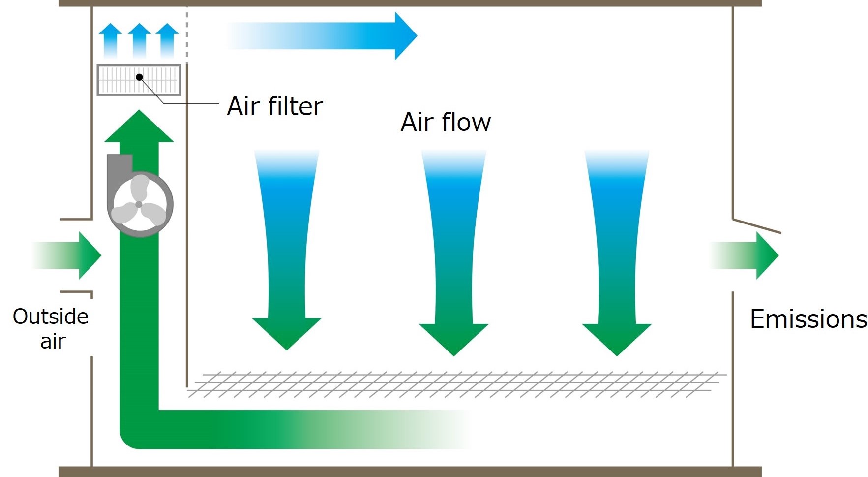
Air pressure in the clean room’s equipment area is also a concern. Controlling the air supplied and removed by the air-conditioning system ensures that the pressure inside the room is maintained at a higher level than in adjacent corridors, shutting off any flow of air from outside to inside. Making good use of the ventilation pressure difference minimizes invading dust.
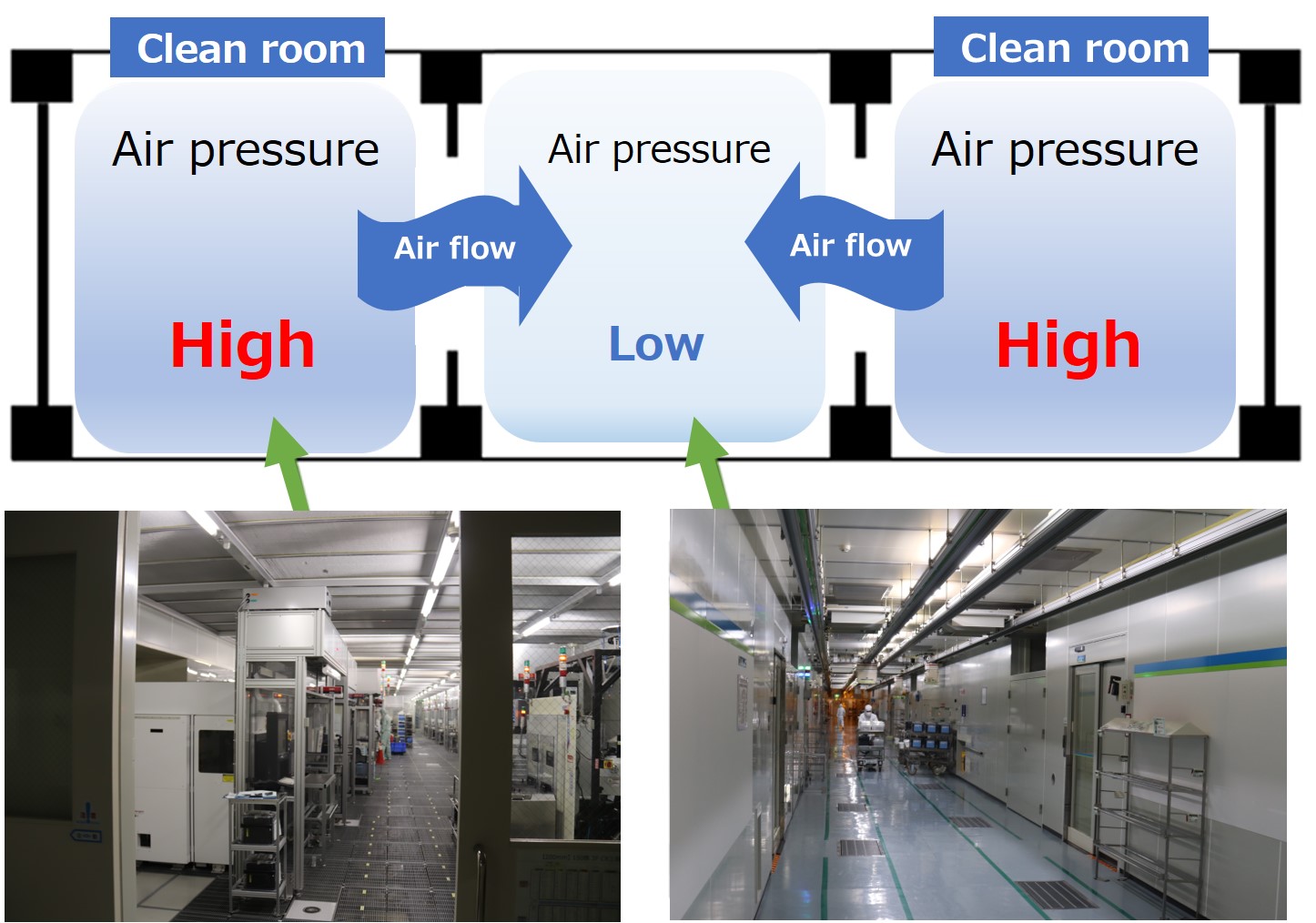
Areas where equipment is located are positively pressure controlled so that the air pressure is higher than in adjacent corridors, even though they are in the same clean room.
On top of all this, since fibers from clothes can also be a source of dust, operators entering clean rooms wear special dustproof coveralls, masks, gloves, and shoes. Before entering the clean room, they wash their gloved hands and use an air towel to blow off the water, step on adhesive sheets on the floor that don’t miss even the smallest specks of dust on the soles of their shoes, and finally walk through an air shower that removes any dust on their coveralls. These thorough procedures maintain cleanliness.
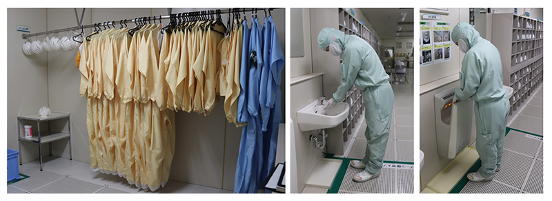
Put on dustproof coveralls in the changing room of the clean room—and don’t forget to wash and dry your hands.
All these various measures are carefully carried out in order to maintain the very highest quality of semiconductor products, but the fact is there’s a lot more that also has to be done to keep the air in the clean rooms clean, and to keep production lines humming along 24 hours a day. That’s the responsibility of the people who carry out maintenance of the manufacturing equipment.
How do you remove minute dust particles that are invisible to the naked eye? And how do you solve equipment problems that cannot be seen from the outside? In the second article we will introduce the day and night struggles of the operators in the clean room.
![]()


Share this article