


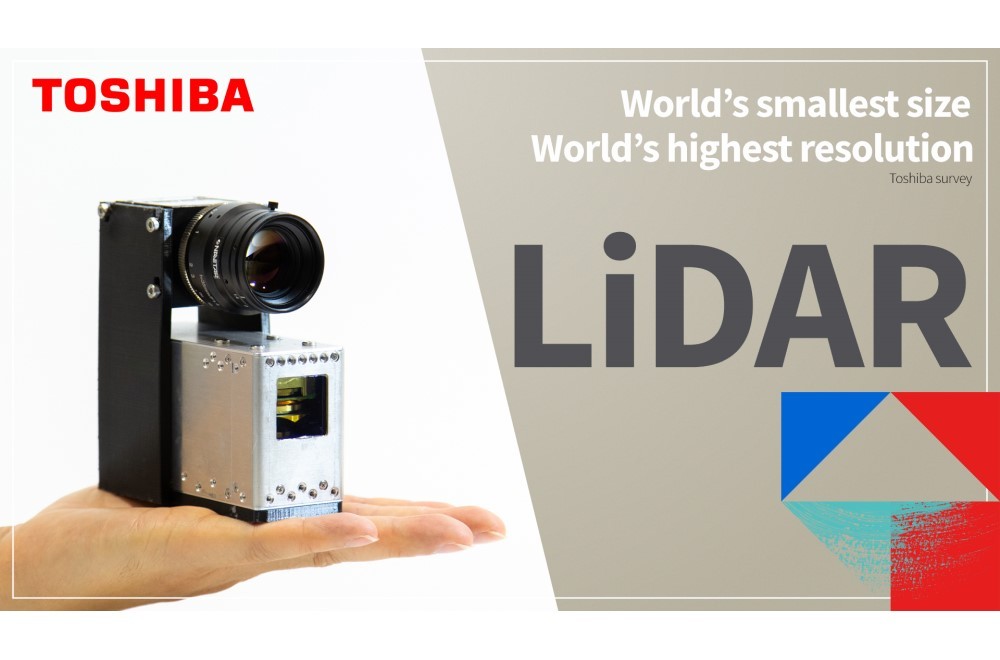
Taking on the World’s Smallest LiDAR, Part 1 –Improving the “Eyes” of Autonomous Driving
2022/03/02 Toshiba Clip Team
- Tech and trends in LiDAR, an essential sensor for autonomous driving
- Can latecomer Toshiba win LiDAR leadership with ultra-miniaturization?
- Overcoming LiDAR weaknesses to achieve low price and high resolution
LiDAR is an essential sensor for automating driving. The technology is already installed in some luxury cars, where it has achieved Level 3, Conditional driving automation, on the six-level scale of standards devised by the Society of Automotive Engineers. In the near future, we can expect to see vehicles that take the next step, to high driving automation of Level 4 and above.
This progress is creating a fast growing market for LiDAR, as revealed in September 2020 figures from French analyst Yole Développement: global demand of US$1.6 billion in 2019 is expected to more than double by 2025, to $3.8 billion; from 171.2 billion yen to 107,406.6 billion yen (at 107 yen to the dollar). This immense potential is attracting major companies and startups alike, all working to install the technology in Level 4 commercial vehicles.
Toshiba is among the companies with a LiDAR that can handle Level 4 autonomous driving. To find out all about it, including what makes it better than other LiDARs, and what benefits it will bring into our lives, we talked to Akihide Sai, Development Team Leader at the Toshiba Research & Development Center’s IoT Edge Laboratory.
Using a laser to instantly capture surroundings in 3D
LiDAR is the tidy acronym derived from light detection and ranging. The light is a laser, and the technology measures distance—range—by firing it at an object and measuring the reflection time. As Sai explains, it has a history that dates back to the 1970s. “LiDAR has long been used during rocket takeoffs and landings, and for cloud observations. In a more familiar setting, it’s also used in distance measuring instruments in golf”
Asked for a basic explanation of how it works, Sai introduces LiDAR’s three core elements: the laser beam source, the light receiver, and its IC chip. The source emits the laser beam, and its reflected signal is detected by the receiving unit. The IC does the work of calculating the time it takes for the beam to bounce back and the distance to the object. As the speed of light is constant, the simple formula of distance = speed x time makes deriving the distance relatively easy.

Akihide Sai, Senior Research Scientist,
IoT Edge Laboratory, Information and Communications Platform Laboratories,
Corporate Research & Development Center, Toshiba Corporation
A laser produces artificial light that is amplified with a resonator. Unlike usual light source, bulbs or LEDs say, the emitted light ray does not spread; instead it forms a very straight, very narrow beam. This makes it ideal for LiDAR, which needs to reach distant targets. Light is part of the electromagnetic spectrum. For example, an electromagnetic wave with a long wavelength is a radio wave that can be used for communications, etc. Far infrared rays that emit heat are in the 10-20 micrometer waveband, and visible light is in the 400-700 nanometer band. As wavelengths further shorten, they become ultraviolet rays, X-rays, and Y-rays.
Most current LiDARs emit 900-nanometer electromagnetic waves as laser beams. Asked if performance could be improved by using a longer wavelength laser with a longer range, Sai explains the current status. “900 nanometers is the mainstream because we have to consider safety, and because we don’t have semiconductors that can output long-wavelength lasers at high power,” It seems it’s not that easy to turn ideas into items on a desk.
Recent generations of LiDAR have added to basic ranging by revealing three-dimensional information about target objects. The laser swings from side to side as it fires, and the numerous small points of light reflected from the object are captured by the light receiver. The grouping they form can be understood as a 3D shape.
In the early 2010s, this ability to scan the shape of target objects coincided with growing excitement about the promise of autonomous driving. Once again the potential of LiDAR was in the news.
“Back then, the mainstream LiDAR used for autonomous driving was mechanical,” explains Sai. “It was a rotating mechanism installed on the vehicle’s roof, and it irradiated lasers through a 360° range. This allowed the surroundings to be understood. The problem with that was that mechanical drive units increase size and cost, and it’s not realistic to install them on commercial vehicles. What was needed was a solid-state LiDAR.”
A solid-state circuit or device utilizes electrical phenomena and has no moving parts. A typical example is the semiconductor. A solid-state LiDAR uses semiconductor technology, integrated circuits, to eliminate mechanical components from laser scanning. Since there are no motors or other mechanical parts, size and price can be reduced, and there is a lot more freedom when it comes to installation.
These pluses mean that the solid-state LiDAR is widely seen as a future mainstream product, even though it still has some disadvantages. Chief among them are that it lacks a rotation mechanism, so cannot cover a full 360°, and that it is not that good at long distance ranging.
Sai explain what this means in real terms. “Current thinking is that achieving Level 4, fully automated driving under specific conditions, with a full understanding of the 360° area around the vehicle, will need six LiDAR in all, five short-to mid-range devices and one long-range LiDAR. For that to happen, we need to see more price reductions and performance improvements. Those are the real challenges current in-vehicle LiDAR needs to overcome.”
The solid-state LiDAR Toshiba developed with it original technologies now realizes those performance improvements.
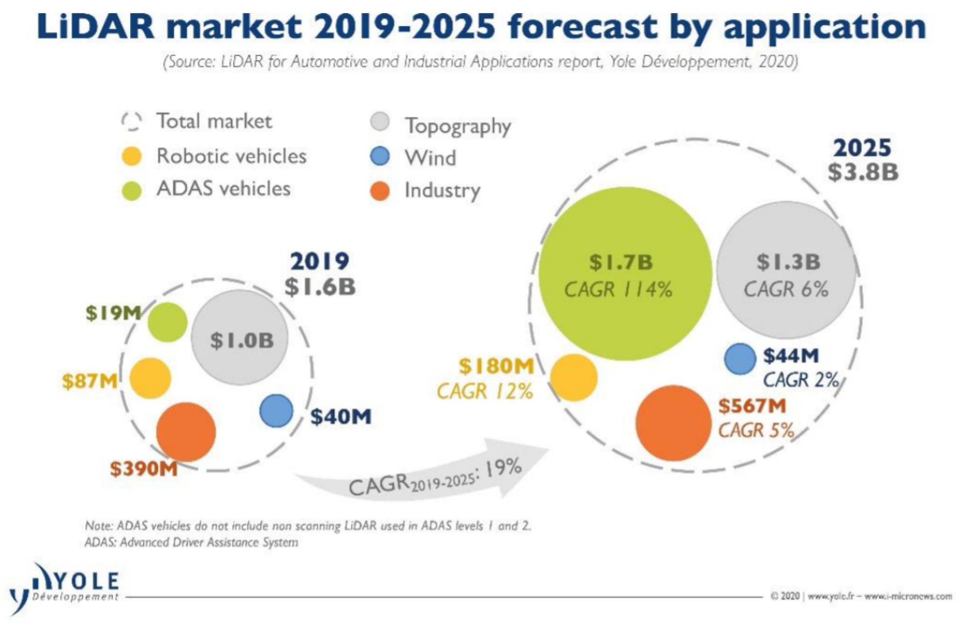
LiDAR Market Forecast by Application (2019-2025)
Source: LiDAR for Automotive and Industrial Applications report, Yole Développement
A market latecomer, but Toshiba brought comprehensive technological capabilities to successful development of an innovative LiDAR
Toshiba’s work on LiDAR development started quite recently, back in 2015. Sai joined the effort a year later, as leader of the solid-state LiDAR development team.
It might not have seemed like the most opportune moment. Tech companies in Silicon Valley had already established leadership in LiDAR, and Sai recalls reports from the west coast of major IT companies carrying out repeated test runs of self-driving cars equipped with their LiDAR.
Toshiba was late to the party, and it’s worth asking why it joined in at all. Of course, there was booming demand for LiDAR, in anticipation of realizing practical autonomous vehicles—but just because the demand is there, that doesn’t mean a company can or should jump into the market. But as Sai explains, there was a good reason: “The solid-state LiDAR required for autonomous driving was a really close fit with technologies Toshiba had cultivated over many years.
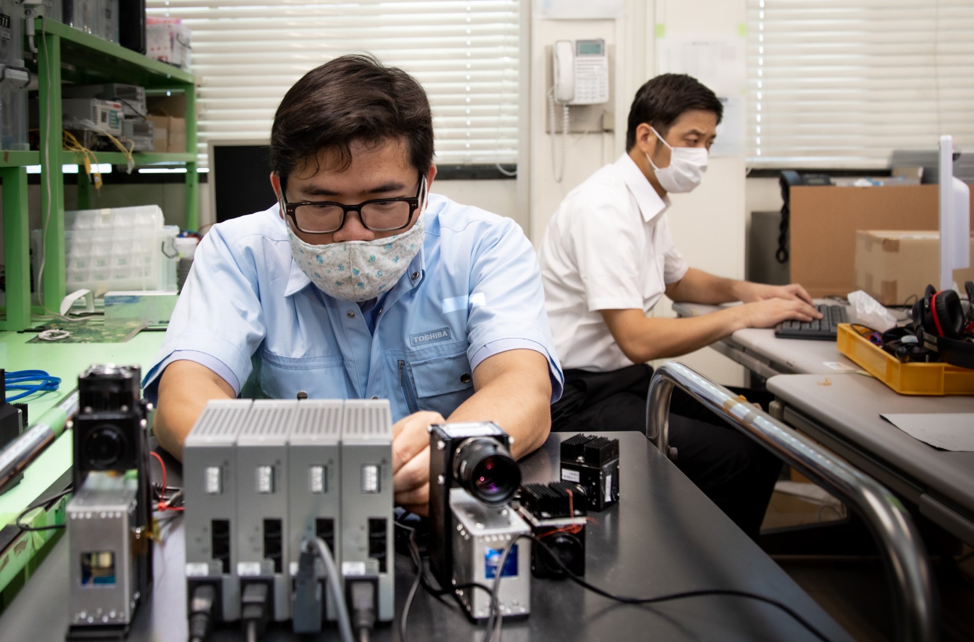
Sai and a colleague in the lab, carrying out a simple ranging test on solid-state LiDAR
Building a solid-state LiDAR, realizing miniaturization and a low cost, relies on semiconductor and optical technologies, both areas where Toshiba has strength. We have decades of experience in semiconductors, and our expertise in optical technologies includes past work on image sensors. Of course, we also have expertise in high density mounting of components. When I think about it, the know-how needed to develop LiDAR is in the DNA of many of our divisions.”
Toshiba’s 2D light receiving array developed compare with a conventional array
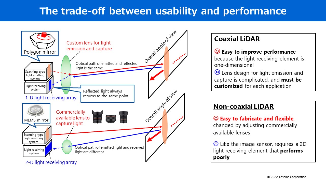
Toshiba found a way forward for the solid-state LiDAR, and set off in its own direction. The basic choice was to develop a non-coaxial LiDAR, suitable for a solid-state solution.
As non-coaxial suggests, there are also coaxial LiDAR systems. These release a laser beam that is reflected back to the receiver along the same optical path. Achieving that requires use of a single scanning lens to emit and receive the beam, and that has to be dedicated custom lens.
In non-coaxial LiDAR systems, the emitted and received beam take different paths, and the lens is used only to receive the signal. This removes the need for a custom lens, and commercially available telephoto or wide-angle lenses can be used, depending on the LiDAR application. This is a major advantage in terms of winning the cost reductions and miniaturization essential for realizing a solid-state LiDAR. It’s also a plus in terms of flexible system configuration that is compatible with a wide range of vehicles and models, opening the way to future installation in all kinds of autonomous vehicles.
“The non-coaxial type receiver has exactly the same mechanism as a camera image sensor,” explains Sai. “Toshiba has an affiliate that has manufactured cameras since way back, so we incorporated a small camera housing for that technology into our LiDAR. That’s also why non-coaxial LiDAR is sometimes called camera-type LiDAR.
While he makes it all sound simple, Sai admits that, once the basic approach was decided on, there were major challenges ahead. “With Toshiba’s non-coaxial solid-state LiDAR it was initially difficult to achieve both high performance long-distance measurements and high resolution”.
The solution to this problem was announced in July 2020: the development of LiDAR light receiving technology that would help to realize advanced autonomous driving of Level 4 and above. This breakthrough achieved a long-distance measurement performance of 200 meters, matching the level of mechanical systems, while also securing high resolution images. As Sai notes, it was an advance that eliminated the weaknesses. So how was it done?
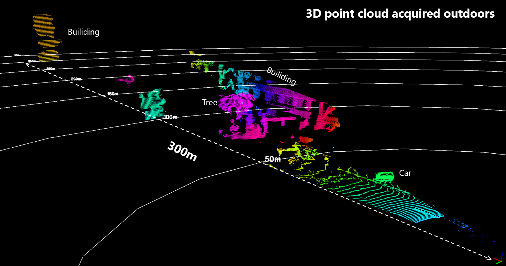
Obstacle detection using Toshiba’s LiDAR delivers the highest resolution in the world while maintaining the longest range, 200m
A technical breakthrough in SiPM, stepping-stone to the world’s smallest LiDAR
The answer is to be found in the silicon photo multiplier (SiPM), a sensor that is highly sensitive to light.
Light is made up of elementary particles, photons. An SiPM is sensitive enough to detect even a faint reflected laser signal, and when it captures a single photon it converts it into a million electrons. The shape of the object reflecting the light can be imaged by using an IC to further convert the electrons into pixels.
The sensitivity, range, and resolution of a LiDAR can be boosted by packing in SiPM, but the downside to doing that is an increase the size of the IC and a larger final product. That leaves developers facing a problem: how to improve performance while maintaining compactness.
“An SiPM is an aggregate of multiple light receiving cells,” explains Sai, “But once a cell is triggered by a photon it needs recovery time, during which it cannot function. To counter this and capture photons without signal loss typically requires mounting a lot of cells in the SiPM, so that there are always cells on standby, available to detect incoming light. However, doing this increases the area occupied by the cells.
“We got around this by installing transistors in the SiPMs that quickly restart the unresponsive light receiving cells. By cutting their recovery time, we have made it possible to detect light continuously without loss, and without increasing the number of SiPMs.
In practice, this approach achieves efficient light detection with a smaller number of light receiving cells, and the SiPM itself is significantly reduced in size. This is what Toshiba calls its “2D SiPM array”. Sai says that this approach has also made it possible to arrange a large number of SiPMs within a limited light receiving area, winning an increase in image resolution.
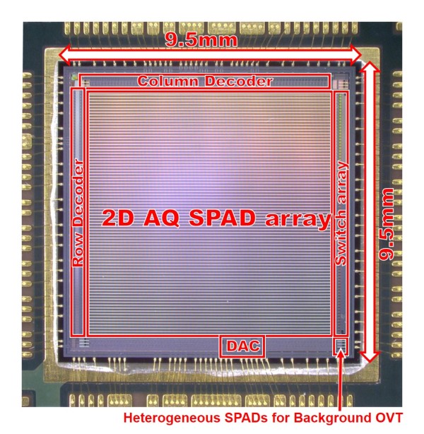
The 2D SiPM array chip developed by Toshiba that contributed to LiDAR miniaturization
These advances grow from the comprehensive strengths Toshiba has cultivated. Within a few years of entering the market, the company announced innovations that moved LiDAR forward. And only a year later came this light receiving technology for LiDAR that will contribute to realizing the high driving automation of Level 4 and beyond. Further advances have now delivered a LiDAR that boasts the world’s smallest size and highest image quality, and a ranging distance of 200m, the longest for a solid-state LiDAR.”
What is the story behind the successful development of LiDAR light receiving technology in just a year? Apart from autonomous driving, what other fields need LiDAR? Part 2 of this article look at how Toshiba’s high-performance solid-state LiDAR will be used on the roads of the future, in logistics, infrastructure.
![]()
![]()

Share this article